

Transmission Electron Microscopy
The transmission electron microscope (TEM) is ideal for studying the defect microstructures of crystals, and probably no other single instrument has contributed more to our understanding of the nature of crystal defects and of microstructurally related properties of a wide range of crystalline materials. In addition to the usual imaging and electron diffraction facilities, most modern microscopes for materials science research are equipped with an x-ray energy dispersive spectrometer (EDS) for chemical analysis of very small regions of specimen. Thus, modern transmission electron microscopy (also TEM) can be considered as a logical development from {optical microscopy, x-ray crystallography, and electron microprobe analysis} techniques with which most mineralogists and geologists are familiar. From “Transmission Electron Microscopy of Minerals and Rocks” by Alex C. McLaren.
TEM uses a static beam of ~2MV electron (typically ~300kV in general labs) to illuminate a desired region (few angstrom to few 10 micrometer diameter) of an electron-transparent specimen which is immersed in the objective lens of the microscope. The transmitted and forward scattered electrons are recombined by the objective lens to from a diffraction pattern in the back focal plane, and a magnified image in the image plane. Using subsequent lenses, either the image of the diffraction pattern is projected onto a fluorescent screen for observation, or digital imaging devices for recording.
Most of the information concerning the internal defect structure, grain morphology, particle shape, etc. may be obtained at reasonable magnifications (~150 kx) and only specific type of observations use the full magnifying capability (~ 1.5Mx).
For example, complete characterization of small particles, either individually isolated or enclosed within a matrix or medium, as in the case of catalyst and asbestos fiber; identifications of small phases and materials such as weathered rocks, soils, and fly ashes; understanding the microstructure and microchemistry of low atomic number, beam sensitive materials such as polymers, biotically formed mineral nanoparticles, and poorly crystallized minerals (transition metal – oxides and hydroxides).
APPLICATIONS
- Revealing submicroscopic microstructure of rock-forming minerals
- Alternating lamellae of orthoclase and twinned albite in a Moonstone
- Brazil and Dauphine twin boundaries in Quartz
- Grain boundaries in synthetic calcite, olivine, basalt, etc.
- Characterizing the internal behavior respoinding to external stimuli
- Micro cracks, dislocations, stacking faults, and other structural defects introduced by deformation
- Diffusive order-disorder transformation in Microcline
- Displacive order-disorder transformation in Anorthoclase
- Assessing the structure and chemistry of nanominerals and mineral nanoparticles
- Platinum group element released from nanoparticles in automobile catalytic converter emissions
- Green rust mineral nanoparticles in contaminant mine drainage from former uranium mine
- Mineral nanoparticles in rock coatings in smelter-impacted area
- Heavy metal nanoparticles in sewage sludge, soil, storm water, plant, etc.
- REE in coal fly ash, coal tailings
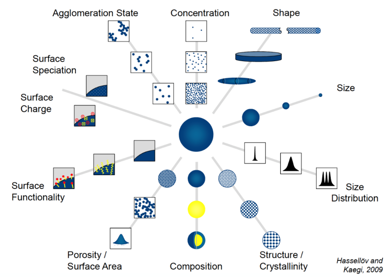
- Evaluating various properties of nanomaterials (see figure below)
From “Analysis and Characterization of Manufactured Nanoparticles in Aquatic Environments” by Martin Hassellöv and Ralf Kaegi, in Environmental and Human Health Impacts of Nanotechnology (Jamie R. Lead and Emma Smith, ed.)
LIMITATIONS
- Specimen needs to be thin (typically thinner than 100nm and less than 50nm for atomic resolution imaging and accurate spectroscopy). Thus, sample preparation could be the most challenging, labor intense and critical step.
- Specimen needs to be mechanically and structurally stable under the high energy electron beam (otherwise causes significant specimen damage by ionization (knock-on) and/or local heating, then creates artifacts).
- TEM images are a 2D projection of 3D specimens. This means that the images, diffraction information, or spectra information obtained by TEM is averaged through the thickness of the specimen, i.e., there is no depth sensitivity in a single TEM data.
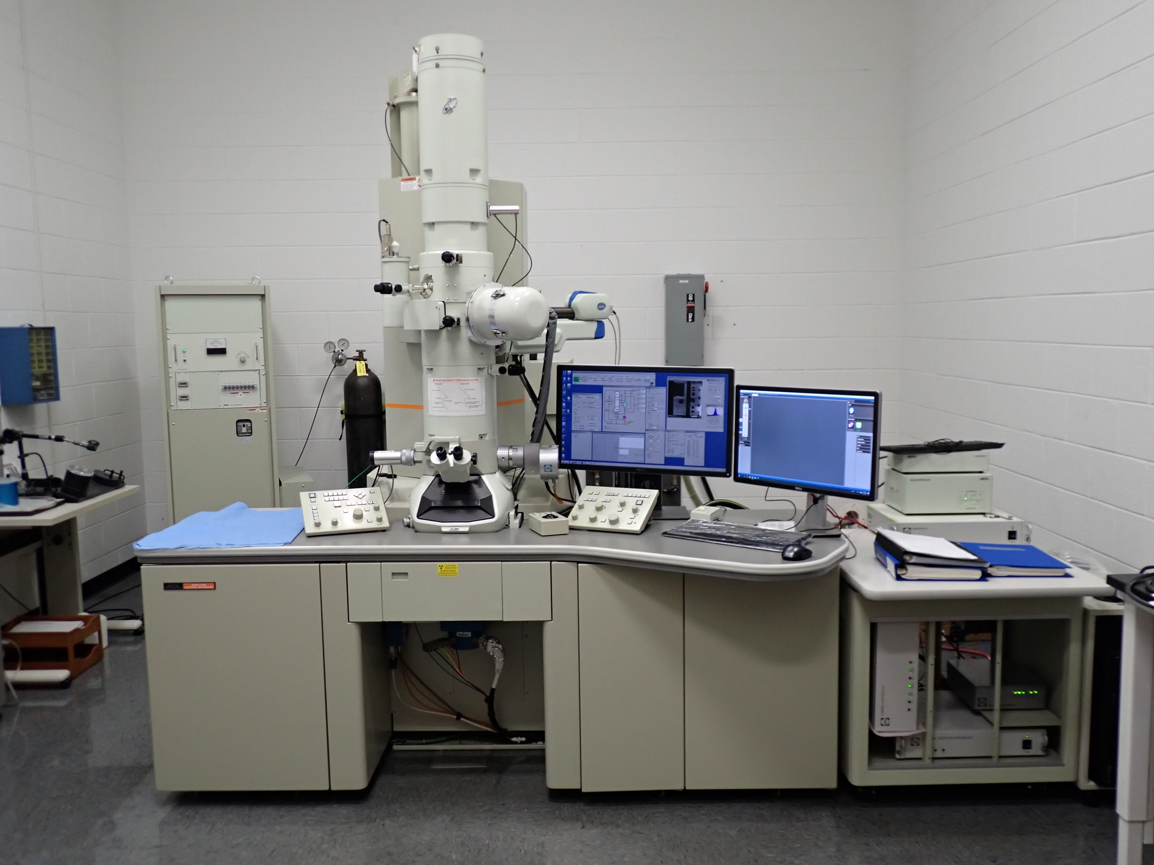
The NCFL has two TEMs:
JEOL JEM 2100: Scanning TEM equipped with HAADF and EDS
The JEOL JEM 2100 TEM is an analytical transmission electron microscope using a LaB6 electron source. This TEM was installed in 2016 for general day-to-day research and research training. TEM has been heavily used due to its STEM-EDS mapping (maximum resolution 5nm) and polymeric and biological samples imaging capabilities.
TECHNICAL SPECIFICATIONS
- JEOL genuine 60mm2 silicon drift Energy Dispersive X-ray (EDS) detector;
- JEOL Bright Field detector for STEM imaging;
- JEOL genuine High Contrast (lower pole-piece) aperture for enhancing image contrast in STEM-BF and TEM for polymeric and biological samples;
- Variable accelerating voltages between 40 and 200kV;
- Gatan Orius 833 slow scan CCD camera (2048 × 2048 pixels) for recording images, electron diffraction patterns and large field of view imaging;
- Gatan Ultrascan 1000XP CCD camera (2048 × 2048 pixels, 14bit) for high resolution imaging (not recommended for SAED);
- Gatan Digital Micrograph ver. 3 (GMS-III);
- Shot Meister (SIF, Japan) package for sequential (montage) imaging;
- Spatial resolution (HRP, 200kV)
- TEM Point-to-Point 0.23nm
- TEM Line 0.14nm
- STEM ~0.3nm (EDS 0.5nm)
Typical applications for this instrument are the imaging of soft and hard materials, diffraction analysis of crystalline materials, STEM-EDS chemical mapping, and general research.
This TEM is used for training, teaching and research/research education. Users can be trained to operate this instrument autonomously. Training for the first-step basic operation consists of 2 × 4-hour sessions (minimum). Additional training sessions will be required for advanced operation, such as EDS mapping, STEM imaging, and other modes.
- Maximum sample size: 3-mm diameter, 150 µm thick (including TEM specimen grid) and materials must be high vacuum compatible
- Biomaterials must be biosafety level 0 (BSL-0) or BSL-1 already prepared on a TEM grid. Toxic or potentially infectious biomaterials are not allowed.
- TEM images are a 2D projection of 3D specimens. This means that the images, diffraction information, or spectra information obtained by TEM is averaged through the thickness of the specimen, i.e., there is no depth sensitivity in a single TEM data. To minimize this projection effect, Observation area needs to be thin and mechanically and structurally stable under the high energy electron beam.
Philips EM420: Thermal emitter (LaB6) TEM
The Philips EM420 is a conventional TEM using a LaB6 electron source; mainly focuses on BF/DF imaging and electron diffraction pattern recording. The microscope is capable low acceleration voltage operation (from 40 up to 120kV), thus it is ideal for polymer, bio and other electron beam sensitive materials. This TEM is also ideal for routine TEM investigations, sample survey and diffraction/imaging experiments require large tilt angles.
TECHNICAL SPECIFICATIONS
- Variable acceleration voltage from 40 to 120 kV (20kV is possible with ultra-thin sample);
- High sample tilt capability ±45°;
- Philips Single tilt multi-specimen holder;
- Philips Double tilt holder;
- SIA-8C slow scan CCD camera (2048 × 2048 pixels, 14bit) for recording images and electron diffraction patterns;
- Spatial resolution (120kV)
- TEM Point-to-Point 0.34nm
- TEM Line 0.1nm 0.20nm
This TEM is used for training, teaching and research/research education. Users can be trained to operate this instrument autonomously. Training for the basic operation consists of 2 × 4-hour sessions (minimum).
- Maximum sample size: 3-mm diameter, 150 µm thick (including TEM specimen grid)
- Biomaterials must be biosafety level 0 (BSL-0) or BSL-1 already prepared on a TEM grid. Toxic or potentially infectious biomaterials are not allowed.
- TEM images are a 2D projection of 3D specimens. This means that the images, diffraction information, or spectra information obtained by TEM is averaged through the thickness of the specimen, i.e., there is no depth sensitivity in a single TEM data. To minimize this projection effect, Observation area needs to be thin and mechanically and structurally stable under the high energy electron beam.
- Estes, E. R., D. Berti, N. R. Coffey, M. F. Hochella Jr., A. S. Wozniak and G. W. Luther III (2019). Abiotic synthesis of graphite in hydrothermal vents. Nature Communications, 10.
- Gartman, A., A.J. Findlay, M. Hannington, D. Garbe-Schonberg, J.W. Jamieson, and T. Kwasnitschka (2019). The role of nanoparticles in mediating element deposition and transport at hydrothermal vents. Geochimica et Cosmochimica Acta, 261, 113-131.
- Rod, K. A., Smith, A. P., Leng, W., Colby, S., Kukkadapu, R. K., Bowden, M., Qafoku, O., Um, W., Hochella, M. F., Jr., Bailey, V. L. and Renslow, R. S. (2020). Water-dispersible nanocolloids and higher temperatures promote the release of carbon from riparian soil. Vadose Zone Journal, 19(1), e20077. https://doi.org/10.1002/vzj2.20077
- Schindler, M., A. J. Lussier, J. Bellrose, S. Rouvimov, P. C. Burns and T. K. Kyser (2017). "Mobilization and agglomeration of uraninite nanoparticles: A nano-mineralogical study of samples from the Matoush Uranium ore deposit." American Mineralogist 102(9): 1776-1787.
- Schindler, M. and D. M. Singer (2017). "Mineral surface coatings: Environmental records at the nanoscale." Elements 13(3): 159-164.
- Schindler M. and Hochella M.F., Jr. (2017) Sequestration of Pb-Zn-Sb- and As-bearing incidental nanoparticles by mineral surface coatings and mineralized organic matter in soils. Environmental Science Processes & Impacts, DOI: 10.1039/C7EM00202E.
- Schindler, M., Berti, D. and Hochella, M.F., Jr. (2017). Previously unknown mineral-nanomineral relationships with important environmental consequences: The case of chromium release from dissolving silicate minerals. American Mineralogist (doi.org/10.2138/am-2017-6170).
- Schindler, M., Lanteigne S., McDonald, A.C. and Hochella, Jr. M.F. (2016). Evidence of Cu- and Ni-bearing surface precipitates and adsorption complexes in remediated soils at the nanoscale: A TEM, micro-Raman and Laser-Ablation ICP-MS study of mineral surface coatings. Canadian Mineralogist 54, 1-25.
- Schindler M; Hochella MF. (2016). Nanomineralogy as a new dimension in understanding elusive geochemical processes in soils: The case of low-solubility-index elements. GEOLOGY, 44(7), 515-518. doi:10.1130/G37774.1
- Schindler, M. and Hochella, M.F., Jr. (2015). Soil memory in mineral surface coatings: Environmental processes recorded at the nanoscale. Geology, 43, 415-418.
- Schlindler, M., Legrand, C.A., and Hochella, M.F., Jr. (2015) Alteration, adsorption and nucleation processes on clay-water interfaces: Mechanisms for the retention of uranium by altered clay surfaces on the nanometer scale. Geochimica et Cosmochimica Acta, 153, 15-36.
- Selkregg, K. (2018) Fusion cast refractories: Role of contaminants. American Ceramic Society Bulletin, 97, 21-28. (http://ceramics.org/wp-content/bulletin/2018/March2018/March2018.html#p=1)
Below are a few videos prepared by Professor Mitsuhiro Murayama for Virginia Tech's NANO 3016 course.
The transmission electron microscope (TEM) is ideal for studying the defect microstructures of crystals, and probably no other single instrument has contributed more to our understanding of the nature of crystal defects and of microstructurally related properties of a wide range of crystalline materials. In addition to the usual imaging and electron diffraction facilities, most modern microscopes for materials science research are equipped with an x-ray energy dispersive spectrometer (EDS) for chemical analysis of very small regions of specimen. Thus, modern transmission electron microscopy (also TEM) can be considered as a logical development from {optical microscopy, x-ray crystallography, and electron microprobe analysis} techniques with which most mineralogists and geologists are familiar. From “Transmission Electron Microscopy of Minerals and Rocks” by Alex C. McLaren.
TEM uses a static beam of ~2MV electron (typically ~300kV in general labs) to illuminate a desired region (few angstrom to few 10 micrometer diameter) of an electron-transparent specimen which is immersed in the objective lens of the microscope. The transmitted and forward scattered electrons are recombined by the objective lens to from a diffraction pattern in the back focal plane, and a magnified image in the image plane. Using subsequent lenses, either the image of the diffraction pattern is projected onto a fluorescent screen for observation, or digital imaging devices for recording.
Most of the information concerning the internal defect structure, grain morphology, particle shape, etc. may be obtained at reasonable magnifications (~150 kx) and only specific type of observations use the full magnifying capability (~ 1.5Mx).
For example, complete characterization of small particles, either individually isolated or enclosed within a matrix or medium, as in the case of catalyst and asbestos fiber; identifications of small phases and materials such as weathered rocks, soils, and fly ashes; understanding the microstructure and microchemistry of low atomic number, beam sensitive materials such as polymers, biotically formed mineral nanoparticles, and poorly crystallized minerals (transition metal – oxides and hydroxides).
APPLICATIONS
- Revealing submicroscopic microstructure of rock-forming minerals
- Alternating lamellae of orthoclase and twinned albite in a Moonstone
- Brazil and Dauphine twin boundaries in Quartz
- Grain boundaries in synthetic calcite, olivine, basalt, etc.
- Characterizing the internal behavior respoinding to external stimuli
- Micro cracks, dislocations, stacking faults, and other structural defects introduced by deformation
- Diffusive order-disorder transformation in Microcline
- Displacive order-disorder transformation in Anorthoclase
- Assessing the structure and chemistry of nanominerals and mineral nanoparticles
- Platinum group element released from nanoparticles in automobile catalytic converter emissions
- Green rust mineral nanoparticles in contaminant mine drainage from former uranium mine
- Mineral nanoparticles in rock coatings in smelter-impacted area
- Heavy metal nanoparticles in sewage sludge, soil, storm water, plant, etc.
- REE in coal fly ash, coal tailings
- Evaluating various properties of nanomaterials (see figure below)
From “Analysis and Characterization of Manufactured Nanoparticles in Aquatic Environments” by Martin Hassellöv and Ralf Kaegi, in Environmental and Human Health Impacts of Nanotechnology (Jamie R. Lead and Emma Smith, ed.)
LIMITATIONS
- Specimen needs to be thin (typically thinner than 100nm and less than 50nm for atomic resolution imaging and accurate spectroscopy). Thus, sample preparation could be the most challenging, labor intense and critical step.
- Specimen needs to be mechanically and structurally stable under the high energy electron beam (otherwise causes significant specimen damage by ionization (knock-on) and/or local heating, then creates artifacts).
- TEM images are a 2D projection of 3D specimens. This means that the images, diffraction information, or spectra information obtained by TEM is averaged through the thickness of the specimen, i.e., there is no depth sensitivity in a single TEM data.
The NCFL has two TEMs:
JEOL JEM 2100: Scanning TEM equipped with HAADF and EDS
The JEOL JEM 2100 TEM is an analytical transmission electron microscope using a LaB6 electron source. This TEM was installed in 2016 for general day-to-day research and research training. TEM has been heavily used due to its STEM-EDS mapping (maximum resolution 5nm) and polymeric and biological samples imaging capabilities.
TECHNICAL SPECIFICATIONS
- JEOL genuine 60mm2 silicon drift Energy Dispersive X-ray (EDS) detector;
- JEOL Bright Field detector for STEM imaging;
- JEOL genuine High Contrast (lower pole-piece) aperture for enhancing image contrast in STEM-BF and TEM for polymeric and biological samples;
- Variable accelerating voltages between 40 and 200kV;
- Gatan Orius 833 slow scan CCD camera (2048 × 2048 pixels) for recording images, electron diffraction patterns and large field of view imaging;
- Gatan Ultrascan 1000XP CCD camera (2048 × 2048 pixels, 14bit) for high resolution imaging (not recommended for SAED);
- Gatan Digital Micrograph ver. 3 (GMS-III);
- Shot Meister (SIF, Japan) package for sequential (montage) imaging;
- Spatial resolution (HRP, 200kV)
- TEM Point-to-Point 0.23nm
- TEM Line 0.14nm
- STEM ~0.3nm (EDS 0.5nm)
Typical applications for this instrument are the imaging of soft and hard materials, diffraction analysis of crystalline materials, STEM-EDS chemical mapping, and general research.
This TEM is used for training, teaching and research/research education. Users can be trained to operate this instrument autonomously. Training for the first-step basic operation consists of 2 × 4-hour sessions (minimum). Additional training sessions will be required for advanced operation, such as EDS mapping, STEM imaging, and other modes.
- Maximum sample size: 3-mm diameter, 150 µm thick (including TEM specimen grid) and materials must be high vacuum compatible
- Biomaterials must be biosafety level 0 (BSL-0) or BSL-1 already prepared on a TEM grid. Toxic or potentially infectious biomaterials are not allowed.
- TEM images are a 2D projection of 3D specimens. This means that the images, diffraction information, or spectra information obtained by TEM is averaged through the thickness of the specimen, i.e., there is no depth sensitivity in a single TEM data. To minimize this projection effect, Observation area needs to be thin and mechanically and structurally stable under the high energy electron beam.
Philips EM420: Thermal emitter (LaB6) TEM
The Philips EM420 is a conventional TEM using a LaB6 electron source; mainly focuses on BF/DF imaging and electron diffraction pattern recording. The microscope is capable low acceleration voltage operation (from 40 up to 120kV), thus it is ideal for polymer, bio and other electron beam sensitive materials. This TEM is also ideal for routine TEM investigations, sample survey and diffraction/imaging experiments require large tilt angles.
TECHNICAL SPECIFICATIONS
- Variable acceleration voltage from 40 to 120 kV (20kV is possible with ultra-thin sample);
- High sample tilt capability ±45°;
- Philips Single tilt multi-specimen holder;
- Philips Double tilt holder;
- SIA-8C slow scan CCD camera (2048 × 2048 pixels, 14bit) for recording images and electron diffraction patterns;
- Spatial resolution (120kV)
- TEM Point-to-Point 0.34nm
- TEM Line 0.1nm 0.20nm
This TEM is used for training, teaching and research/research education. Users can be trained to operate this instrument autonomously. Training for the basic operation consists of 2 × 4-hour sessions (minimum).
- Maximum sample size: 3-mm diameter, 150 µm thick (including TEM specimen grid)
- Biomaterials must be biosafety level 0 (BSL-0) or BSL-1 already prepared on a TEM grid. Toxic or potentially infectious biomaterials are not allowed.
- TEM images are a 2D projection of 3D specimens. This means that the images, diffraction information, or spectra information obtained by TEM is averaged through the thickness of the specimen, i.e., there is no depth sensitivity in a single TEM data. To minimize this projection effect, Observation area needs to be thin and mechanically and structurally stable under the high energy electron beam.
- Estes, E. R., D. Berti, N. R. Coffey, M. F. Hochella Jr., A. S. Wozniak and G. W. Luther III (2019). Abiotic synthesis of graphite in hydrothermal vents. Nature Communications, 10.
- Gartman, A., A.J. Findlay, M. Hannington, D. Garbe-Schonberg, J.W. Jamieson, and T. Kwasnitschka (2019). The role of nanoparticles in mediating element deposition and transport at hydrothermal vents. Geochimica et Cosmochimica Acta, 261, 113-131.
- Rod, K. A., Smith, A. P., Leng, W., Colby, S., Kukkadapu, R. K., Bowden, M., Qafoku, O., Um, W., Hochella, M. F., Jr., Bailey, V. L. and Renslow, R. S. (2020). Water-dispersible nanocolloids and higher temperatures promote the release of carbon from riparian soil. Vadose Zone Journal, 19(1), e20077. https://doi.org/10.1002/vzj2.20077
- Schindler, M., A. J. Lussier, J. Bellrose, S. Rouvimov, P. C. Burns and T. K. Kyser (2017). "Mobilization and agglomeration of uraninite nanoparticles: A nano-mineralogical study of samples from the Matoush Uranium ore deposit." American Mineralogist 102(9): 1776-1787.
- Schindler, M. and D. M. Singer (2017). "Mineral surface coatings: Environmental records at the nanoscale." Elements 13(3): 159-164.
- Schindler M. and Hochella M.F., Jr. (2017) Sequestration of Pb-Zn-Sb- and As-bearing incidental nanoparticles by mineral surface coatings and mineralized organic matter in soils. Environmental Science Processes & Impacts, DOI: 10.1039/C7EM00202E.
- Schindler, M., Berti, D. and Hochella, M.F., Jr. (2017). Previously unknown mineral-nanomineral relationships with important environmental consequences: The case of chromium release from dissolving silicate minerals. American Mineralogist (doi.org/10.2138/am-2017-6170).
- Schindler, M., Lanteigne S., McDonald, A.C. and Hochella, Jr. M.F. (2016). Evidence of Cu- and Ni-bearing surface precipitates and adsorption complexes in remediated soils at the nanoscale: A TEM, micro-Raman and Laser-Ablation ICP-MS study of mineral surface coatings. Canadian Mineralogist 54, 1-25.
- Schindler M; Hochella MF. (2016). Nanomineralogy as a new dimension in understanding elusive geochemical processes in soils: The case of low-solubility-index elements. GEOLOGY, 44(7), 515-518. doi:10.1130/G37774.1
- Schindler, M. and Hochella, M.F., Jr. (2015). Soil memory in mineral surface coatings: Environmental processes recorded at the nanoscale. Geology, 43, 415-418.
- Schlindler, M., Legrand, C.A., and Hochella, M.F., Jr. (2015) Alteration, adsorption and nucleation processes on clay-water interfaces: Mechanisms for the retention of uranium by altered clay surfaces on the nanometer scale. Geochimica et Cosmochimica Acta, 153, 15-36.
- Selkregg, K. (2018) Fusion cast refractories: Role of contaminants. American Ceramic Society Bulletin, 97, 21-28. (http://ceramics.org/wp-content/bulletin/2018/March2018/March2018.html#p=1)
Below are a few videos prepared by Professor Mitsuhiro Murayama for Virginia Tech's NANO 3016 course.