

Scanning Electron Microscopy
Scanning electron microscope (SEM) is widely used to characterize the sample surface and near-surface. It provides high resolution images, and elemental microanalysis in conjunction with an Energy Dispersive X-ray Spectroscopy (EDS) detector. With specialized instruments and compartments, SEM may have variable pressure or environmental capabilities that specimens can be observed in high vacuum, low vacuum or wet condition; in-situ experiments such as hydrating, dehydrating and sample heating are also possible.
APPLICATIONS
- High resolution imaging of surface topography
- Chemical analysis of nearly the entire period table
- Imaging of insulating and hydrated samples in certain mode
- In-situ experiments such as hydrating, dehydrating and heating
LIMITATIONS
- Sample size restriction
- Ultimate resolution is affected by the sample chemical and stability in the electron beam
Capability: Electron Backscatter Diffraction (EBSD)
Electron backscatter diffraction (EBSD) is a scanning electron microscope–based microstructural-crystallographic characterization technique commonly used in the study of crystalline or polycrystalline materials. The technique can provide information about the structure, crystal orientation, phase, or strain in the material. Traditionally these types of studies have been carried out using X-ray diffraction (XRD), neutron diffraction and/or electron diffraction in a Transmission electron microscope.
The NCFL has three SEMs:
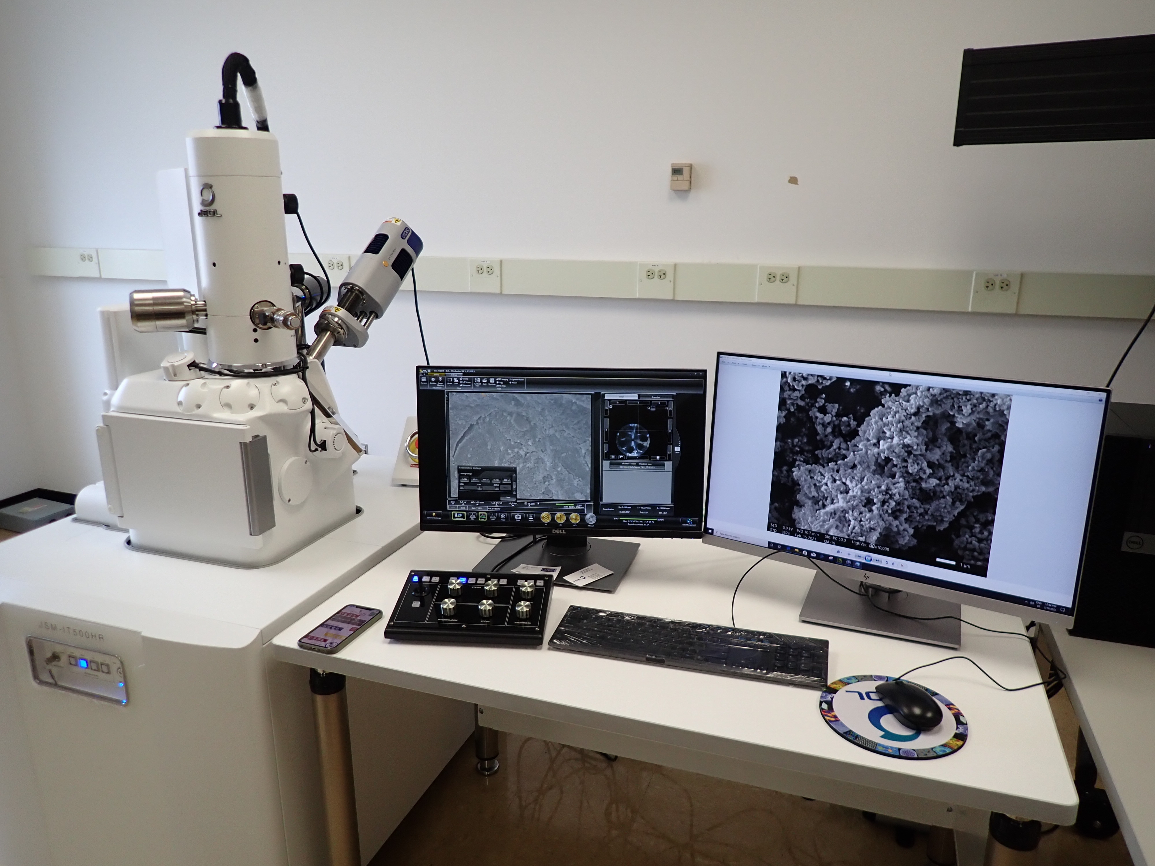
JEOL IT-500HR
JEOL IT-500HR is a newly installed state-of-the-art analytical scanning electron microscope using a Schottky field emission (FEG) electron source. The most attractive features of this instrument are a seamless link from optical to high magnification SEM images and automated large area imaging and spectroscopy analyses. It is also capable of both low acceleration voltage (0.5kV) and high resolution (1.5nm) imaging.
TECHNICAL SPECIFICATIONS
- Accelerating voltage: 500V to 30kV
- Operating pressure: High-vacuum, Low-vacuum up to 150Pa
- Detectors: 1 × Everhart-Thornley (SED) for secondary electron imaging, 1 × Multi-segment solid state backscattered electron detector (BSED) for composition, topographic and variable shadow imaging
- Magnification: ×14 to ×1,680,000 (display 358mm × 269mm)
- Energy Dispersive X-ray Spectroscopy (EDS): Oxford Instruments, AZtecLive Automated Microanalysis System with UltimMax100 (100mm2) Silicon Drift Detector (SDD), Energy Resolution Mn K - 127eV at 130,000 cps.
- Surface imaging, analysis and metrology software: Digital Surf- MountainsMap SEM (Contour, Basic Surface Texture, Color Image Overlay, Colocalization, Surface Stitching, SEM)
- Stage Travel: X= 125mm, Y= 100mm, Z= 5-80mm continuous, Tilt=-10° to +90°, R=360°
- Compatible with Kammrath Weiss tensile module
- Spatial resolution
- High-Vacuum
- 1.5nm at 30kV
- 4.0nm at 1kV
- Low-vacuum
- 1.8nm at 15kV
- High-Vacuum
FEI Quanta 600 FEG: Environmental SEM equipped with EDS, heating stage, mechanical testing fixture
The FEI Quanta 600 FEG is an environmental SEM using a Schottky field emission (FEG) electron source that can operate in high-vacuum, low-vacuum and extended-vacuum modes. It is used to image samples that are difficult to impossible to image in standard high vacuum SEMs; the SEM can operate with pressures around the sample up to 4000 Pa and in conjunction with a Peltier stage can image fully hydrated samples, a critical advantage for imaging biological samples. in situ experiments such as hydrating, dehydrating and heating samples are possible with this ESEM.
TECHNICAL SPECIFICATIONS
- Accelerating voltage: 200V to 30kV
- Probe current: up to 100nA continuously adjustable
- Operating pressure: High-vacuum 6 ×10⁻⁴ Pa, Low-vacuum 10 to 130 Pa, ESEM-vacuum 10 to 4000 Pa
- Detectors: 1 × Everhart-Thornley SED, 1 × Low-vacuum SED (LFD), 1 × Gaseous SED (GSED), 1 × Solid-state BSED, 1 × Gaseous BSED, 1 × IR-CCD
- Energy Dispersive X-ray Spectroscopy (EDS): Bruker QUANTAX 400 with XFlash 4010 (10mm2) Silicon Drift Detector (SDD), Energy Resolution Mn K - 125eV at over 100,000 cps, detection B ~ Am
- Stage Travel: X = Y = 150mm, Z = 65mm (Z clearance 93.5mm), Tilt = -5° to +70° degrees (WD dependent), R = 360° continuous
- Compatible with i) Heating stage ~1000°C and ii) Kammrath Weiss tensile module
- Spatial resolution
- High-vacuum
- 1.2nm at 30kV (SE)
- 2.5nm at 30kV (BSE)
- 3.0nm at 1kV (SE)
- Low-vacuum
- 1.5nm at 30kV (SE)
- 2.5nm at 30kV (BSE)
- 3.0nm at 3kV (SE)
- Extended vacuum mode (ESEM)
- 1.5nm at 30kV (SE)
- High-vacuum
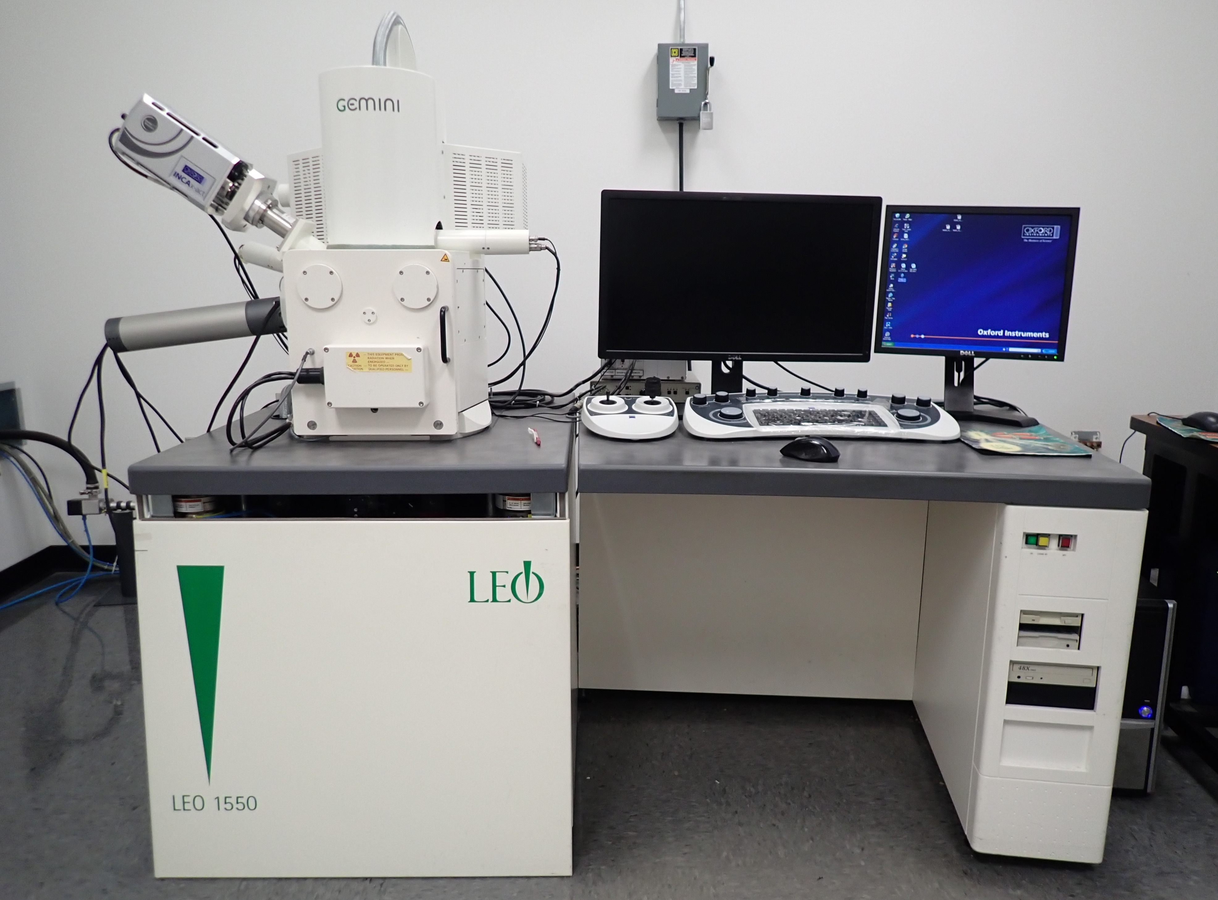
LEO (Zeiss) 1550: Field Emission SEM equipped with EDS and EBSD
The LEO (Zeiss) 1550 is a high-spatial resolution SEM using a Schottky field emission (FEG) electron source, capable of resolution in 1-5 nm size range using an in-lens SED. It is used for high-resolution imaging of surfaces, qualitative assessment of the distribution of elements (by EDS), submicron structure analysis, and determination of crystal orientation and crystalline texture (by EBSD).
TECHNICAL SPECIFICATIONS
- Accelerating voltage: 100V to 30kV
- Detectors: 1 × In-lens secondary electron (SED), 1 x Everhart-Thornley secondary electron (SED), 1 × Robinson-type back-scatter electron (BSED)
- Secondary & backscattered electrons and x-rays, light (for Cathodoluminescence) and Electron Beam Induced current (EBIC)
- Energy Dispersive X-ray Spectroscopy (EDS): Oxford INCA Energy E2H with INCAx-act 51-1385-005 Silicon Drift detector (SDD), Energy Resolution Mn K – 133eV, detection B - U, 0.1 - 1 at%
- HKL Nordlys II Electron Back Scatter Diffraction (EBSD) system, including a Forward Scatter Electron (FSE) detector
- Spatial resolution
- High-vacuum
- 1.0nm at 20kV
- 2.5nm at 1kV
- High-vacuum
NOTE: the effectiveness of low Accelerating voltage operation depends heavily on the nature of a sample.
Coming soon...
Coming soon...