

Raman Spectroscopy
Raman Spectroscopy is a non-destructive chemical analysis technique which provides detailed information about chemical structure, phase and polymorphy, crystallinity and molecular interactions. It is based upon the interaction of light with the chemical bonds within a material.
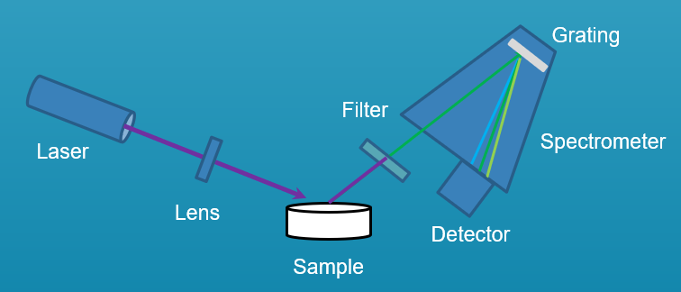
Raman is a light scattering technique, whereby a molecule scatters incident light from a high intensity laser light source. Most of the light is scattered at the same wavelength as the laser source and does not provide useful information – this is called Rayleigh Scattering. However a small amount of light (typically less than 1 in 1 million incident photons) is scattered at different wavelengths, which depend on the chemical structure of the analyte – this is called Raman Scattering which occurs in two ways. If the scattered light is of lower frequency (longer wavelength) than the incident laser, then it is called Stokes scattering. If it is of higher frequency (shorter wavelength), then it is called anti-Stokes scattering. Most Raman spectroscopy detects the more intense Stokes scattering.
APPLICATIONS
- Mineral identification
- Fluid inclusions
- Mineral behaviour under extreme conditions (heating, pressure etc.)
- Identification of airborne particles
- Particle tracking
- Surface-enhanced Raman based sensors
- Plastic particle characterization
- Surface analysis
- Carbon material characterization
- Crystalline structure identification
LIMITATIONS
- The Raman scattering is typically very weak (~ 1 in 10 million incident photons), it needs a sensitive and highly optimized instrumentation
- Can’t be used for metals or alloys
- Thermal heating through the intense laser radiation can either destroy the sample or effect the Raman signals
- Typically can’t quantitatively analyze a solid sample unless the analyte is uniformly distributed
- Fluorescence background (much more intense than the Raman signals) can limit Raman usefulness
WITec alpha500 Raman-AFM Microscope
The WITec alpha500 combines Confocal Raman Microscopy for 3-D Chemical Imaging and Atomic Force Microscopy for high resolution structural imaging in an automated system. It not only allows high resolution surface topography imaging with AFM at many different sample positions but also Raman Imaging, large area Raman scans and multi-point spectra acquisition at a user-defined number of measurement points. The Raman and AFM images of the same sample positions can then be matched and linked together for a comprehensive understanding of the sample's properties.
TECHNICAL SPECIFICATIONS
- 3 Lasers excitation sources (532 nm, 633 nm and 785 nm) with a multi-laser coupling unit for a maximum of experimental flexibility
- Multiple objective selections including air (10x, 20x, 50x and 100x), water immersion (63x) and oil immersion (100x) objectives
- A piezo stage (200 μm x 200 μm) coupled with a motorized microscope stage (10 cm x 15 cm) to allow for high-resolution confocal Raman mapping and large area investigations
- Polarization dependent measurements
- Research-grade optical microscope body with LED Köhler white-light illumination and video camera sample view
- AFM mode: contact, AC and Pulsed Forced mode
Project 1: Aerosol Emission from Fuse-Deposition Modeling 3D Printers in a Chamber and in Real Indoor Environments (Linsey Marr, Co-PI)
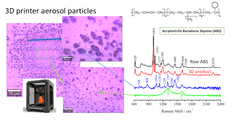
Three-dimensional (3D) printers are known to emit aerosols, but questions remain about their composition and the fundamental processes driving emissions. The objective of this work was to characterize the aerosol emissions from the operation of a fuse-deposition modeling 3D printer. We modeled the time- and size-resolved emissions of submicrometer aerosols from the printer in a chamber study, gained insight into the chemical composition of emitted aerosols using Raman spectroscopy, and measured the potential for exposure to the aerosols generated by 3D printers under real-use conditions in a variety of indoor environments. The average aerosol emission rates ranged from ∼108 to ∼1011 particles min–1, and the rates varied over the course of a print job. Acrylonitrile butadiene styrene (ABS) filaments generated the largest number of aerosols, and wood-infused polylactic acid (PLA) filaments generated the smallest amount. The emission factors ranged from 6 × 10⁸ to 6 × 10¹¹ per gram of printed part, depending on the type of filament used. For ABS, the Raman spectra of the filament and the printed part were indistinguishable, while the aerosol spectra lacked important peaks corresponding to styrene and acrylonitrile, which are both present in ABS. This observation suggests that aerosols are not a result of volatilization and subsequent nucleation of ABS or direct release of ABS aerosols.
Figure 1. Optical images of (a) value ABS aerosols impacted onto a silicon wafer and insets with (b) larger (≥10 µm) and (c) smaller (≤1 µm) aerosols; (d) resulting Raman spectra. Broader peaks are associated with smaller aerosols in (c). Peaks associated with the benzene ring present in styrene are located at 620, 1001, 1031, 1157, and 1183 cm-1. Peak associated with the carbon-nitrogen triple bond in acrylonitrile is located at 2236 cm-1.
Vance, M. E., Pegues, V., Van Montfrans, S., Leng, W., Marr, L. C. (2017). Aerosol Emission from Fuse-Deposition Modeling 3D Printers in a Chamber and in Real Indoor Environments, ES&T, 51(17), 9516-9523.
Coming soon...
Raman Spectroscopy is a non-destructive chemical analysis technique which provides detailed information about chemical structure, phase and polymorphy, crystallinity and molecular interactions. It is based upon the interaction of light with the chemical bonds within a material.
Raman is a light scattering technique, whereby a molecule scatters incident light from a high intensity laser light source. Most of the light is scattered at the same wavelength as the laser source and does not provide useful information – this is called Rayleigh Scattering. However a small amount of light (typically less than 1 in 1 million incident photons) is scattered at different wavelengths, which depend on the chemical structure of the analyte – this is called Raman Scattering which occurs in two ways. If the scattered light is of lower frequency (longer wavelength) than the incident laser, then it is called Stokes scattering. If it is of higher frequency (shorter wavelength), then it is called anti-Stokes scattering. Most Raman spectroscopy detects the more intense Stokes scattering.
APPLICATIONS
- Mineral identification
- Fluid inclusions
- Mineral behaviour under extreme conditions (heating, pressure etc.)
- Identification of airborne particles
- Particle tracking
- Surface-enhanced Raman based sensors
- Plastic particle characterization
- Surface analysis
- Carbon material characterization
- Crystalline structure identification
LIMITATIONS
- The Raman scattering is typically very weak (~ 1 in 10 million incident photons), it needs a sensitive and highly optimized instrumentation
- Can’t be used for metals or alloys
- Thermal heating through the intense laser radiation can either destroy the sample or effect the Raman signals
- Typically can’t quantitatively analyze a solid sample unless the analyte is uniformly distributed
- Fluorescence background (much more intense than the Raman signals) can limit Raman usefulness
WITec alpha500 Raman-AFM Microscope
The WITec alpha500 combines Confocal Raman Microscopy for 3-D Chemical Imaging and Atomic Force Microscopy for high resolution structural imaging in an automated system. It not only allows high resolution surface topography imaging with AFM at many different sample positions but also Raman Imaging, large area Raman scans and multi-point spectra acquisition at a user-defined number of measurement points. The Raman and AFM images of the same sample positions can then be matched and linked together for a comprehensive understanding of the sample's properties.
TECHNICAL SPECIFICATIONS
- 3 Lasers excitation sources (532 nm, 633 nm and 785 nm) with a multi-laser coupling unit for a maximum of experimental flexibility
- Multiple objective selections including air (10x, 20x, 50x and 100x), water immersion (63x) and oil immersion (100x) objectives
- A piezo stage (200 μm x 200 μm) coupled with a motorized microscope stage (10 cm x 15 cm) to allow for high-resolution confocal Raman mapping and large area investigations
- Polarization dependent measurements
- Research-grade optical microscope body with LED Köhler white-light illumination and video camera sample view
- AFM mode: contact, AC and Pulsed Forced mode
Project 1: Aerosol Emission from Fuse-Deposition Modeling 3D Printers in a Chamber and in Real Indoor Environments (Linsey Marr, Co-PI)
Three-dimensional (3D) printers are known to emit aerosols, but questions remain about their composition and the fundamental processes driving emissions. The objective of this work was to characterize the aerosol emissions from the operation of a fuse-deposition modeling 3D printer. We modeled the time- and size-resolved emissions of submicrometer aerosols from the printer in a chamber study, gained insight into the chemical composition of emitted aerosols using Raman spectroscopy, and measured the potential for exposure to the aerosols generated by 3D printers under real-use conditions in a variety of indoor environments. The average aerosol emission rates ranged from ∼108 to ∼1011 particles min–1, and the rates varied over the course of a print job. Acrylonitrile butadiene styrene (ABS) filaments generated the largest number of aerosols, and wood-infused polylactic acid (PLA) filaments generated the smallest amount. The emission factors ranged from 6 × 10⁸ to 6 × 10¹¹ per gram of printed part, depending on the type of filament used. For ABS, the Raman spectra of the filament and the printed part were indistinguishable, while the aerosol spectra lacked important peaks corresponding to styrene and acrylonitrile, which are both present in ABS. This observation suggests that aerosols are not a result of volatilization and subsequent nucleation of ABS or direct release of ABS aerosols.
Figure 1. Optical images of (a) value ABS aerosols impacted onto a silicon wafer and insets with (b) larger (≥10 µm) and (c) smaller (≤1 µm) aerosols; (d) resulting Raman spectra. Broader peaks are associated with smaller aerosols in (c). Peaks associated with the benzene ring present in styrene are located at 620, 1001, 1031, 1157, and 1183 cm-1. Peak associated with the carbon-nitrogen triple bond in acrylonitrile is located at 2236 cm-1.
Vance, M. E., Pegues, V., Van Montfrans, S., Leng, W., Marr, L. C. (2017). Aerosol Emission from Fuse-Deposition Modeling 3D Printers in a Chamber and in Real Indoor Environments, ES&T, 51(17), 9516-9523.
Coming soon...