

Focused Ion Beam
APPLICATIONS
Dual beam FIB-SEM is a workstation that combines a scanning electron microscope (SEM) and a focused ion beam (FIB); it is heavily used in semiconductor industry, materials science, and increasingly in geoscience and biological field for site-specific analysis. SEM delivers high resolution images, while FIB is mostly used to add and subtract micro volumes of material in a controlled manner, like a nanomachining device. Coupled to an Energy Dispersive X-ray Spectroscopy (EDS) detector and Electron Backscattered diffraction (EBSD) camera, dual beam FIB-SEM provides elemental identification and crystallographic properties from the cross-section of the sample. With serial slicing technique, structural, chemical and crystallographic information can be revealed in three dimensions.
- High resolution cross-section images
- Site-specific liftout preparation for TEM analysis
- Grain contrast imaging
- Circuit modification
- Serial slicing and 3D reconstruction
LIMITATIONS
- Vacuum compatibility required
- Sample size restriction
- Ion implantation
- Ion beam damage
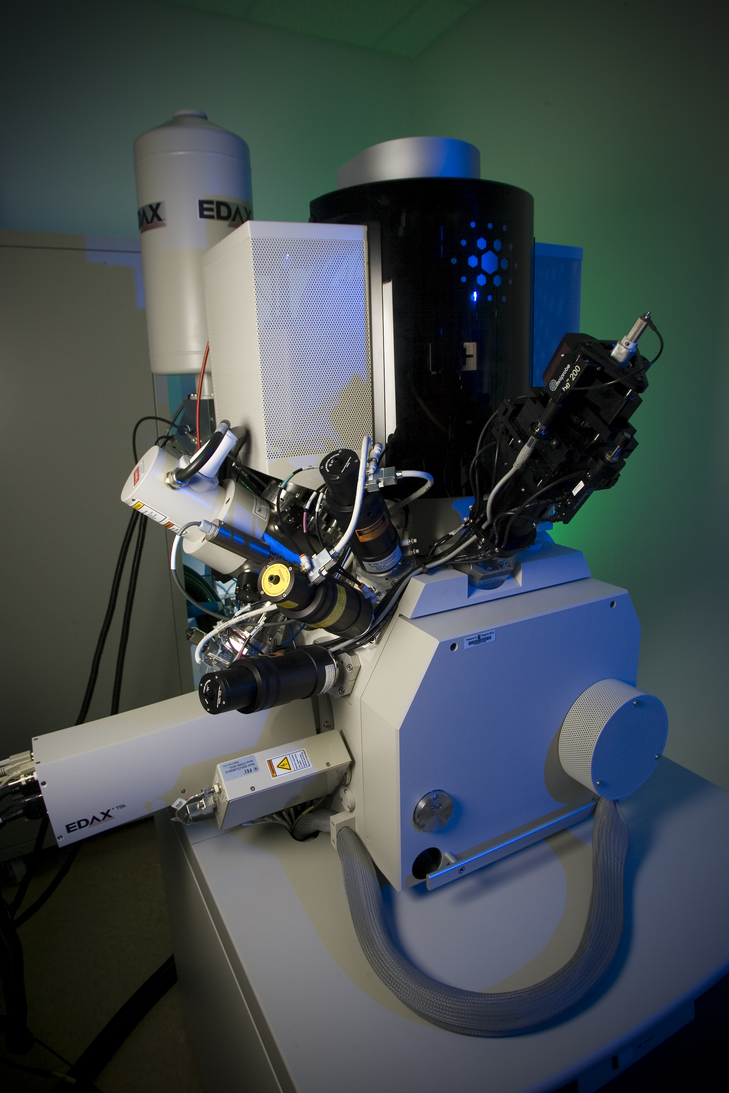
FEI Helios 600 NanoLab: A dual-beam workstation equipped with EDS and EBSD
The FEI Helios 600 NanoLab is a dual-beam workstation that combines a high-resolution SEM and a focused ion beam. It is used to dissect or deposit material at a micro- to nano-meter size scale. The instrument is capable of nanoscale lithography, deposition, and tomography, and it has a manipulator for precisely probing, straining, picking up and placing nanometer sized objects cut from or deposited on a larger samples. It is equipped with an integrated Energy Dispersive Spectrometer (EDS) and Electron Backscatter Diffration (EBSD) package for gathering chemical, spatial orientation, and strain state information. When this package is coordinated with material removal via the ion beam, it is possible to create 3-dimensional reconstructions of the internal structure, chemistry, orientation, and strain state in objects a few nanometers in size. Samples can be studied and handled from room temperature down to cryogenic temperatures.
The NCFL’s Helios 600 NanoLab is equipped with:
- an Omniprobe 200.2
- a 3-nozzle gas injection system with gases for platinum deposition, insulaotor enhanced etching, and selective carbon milling – automated focussed-ion beam milling
- a TEM sample preparation kit
- a STEM detector
- Pegasus XM 4 Integrated EDS and EBSD (Genesis EDS x-ray microanalysis system and Hikari camera for EBSD) with integrated 3D OIM automated data aquisition and batch processing software
- Evactron plasma cleaner and cryo-can
- a lithography package (for electron- or ion-beam lithography) with an electrostatic beam blanker and Nabity pattern generation system
- a Quorum cryo-transfer system
- Amira software license
- a 52-pin electrical feedthrough for custom experiments
TECHNICAL SPECIFICATIONS
- Signals Detected: Electrons, secondary ions, X-rays, light (Cathodoluminescence)
- Imaging/Mapping: Yes
- Lateral Resolution/Probe Size: 7 nm (ion beam); 20 nm (electron beam)
Schindler, M., Michel, S., Batcheldor, D., & Hochella Jr., M.F. (2019). A nanoscale study of the formation of Fe-(hydr)oxides in a volcanic regolith: Implications for the understanding of soil forming processes on Earth and Mars. Geochimica et Cosmochimica Acta, 264, 43–66.
Training modules, videos, sample prep, etc.
APPLICATIONS
Dual beam FIB-SEM is a workstation that combines a scanning electron microscope (SEM) and a focused ion beam (FIB); it is heavily used in semiconductor industry, materials science, and increasingly in geoscience and biological field for site-specific analysis. SEM delivers high resolution images, while FIB is mostly used to add and subtract micro volumes of material in a controlled manner, like a nanomachining device. Coupled to an Energy Dispersive X-ray Spectroscopy (EDS) detector and Electron Backscattered diffraction (EBSD) camera, dual beam FIB-SEM provides elemental identification and crystallographic properties from the cross-section of the sample. With serial slicing technique, structural, chemical and crystallographic information can be revealed in three dimensions.
- High resolution cross-section images
- Site-specific liftout preparation for TEM analysis
- Grain contrast imaging
- Circuit modification
- Serial slicing and 3D reconstruction
LIMITATIONS
- Vacuum compatibility required
- Sample size restriction
- Ion implantation
- Ion beam damage
FEI Helios 600 NanoLab: A dual-beam workstation equipped with EDS and EBSD
The FEI Helios 600 NanoLab is a dual-beam workstation that combines a high-resolution SEM and a focused ion beam. It is used to dissect or deposit material at a micro- to nano-meter size scale. The instrument is capable of nanoscale lithography, deposition, and tomography, and it has a manipulator for precisely probing, straining, picking up and placing nanometer sized objects cut from or deposited on a larger samples. It is equipped with an integrated Energy Dispersive Spectrometer (EDS) and Electron Backscatter Diffration (EBSD) package for gathering chemical, spatial orientation, and strain state information. When this package is coordinated with material removal via the ion beam, it is possible to create 3-dimensional reconstructions of the internal structure, chemistry, orientation, and strain state in objects a few nanometers in size. Samples can be studied and handled from room temperature down to cryogenic temperatures.
The NCFL’s Helios 600 NanoLab is equipped with:
- an Omniprobe 200.2
- a 3-nozzle gas injection system with gases for platinum deposition, insulaotor enhanced etching, and selective carbon milling – automated focussed-ion beam milling
- a TEM sample preparation kit
- a STEM detector
- Pegasus XM 4 Integrated EDS and EBSD (Genesis EDS x-ray microanalysis system and Hikari camera for EBSD) with integrated 3D OIM automated data aquisition and batch processing software
- Evactron plasma cleaner and cryo-can
- a lithography package (for electron- or ion-beam lithography) with an electrostatic beam blanker and Nabity pattern generation system
- a Quorum cryo-transfer system
- Amira software license
- a 52-pin electrical feedthrough for custom experiments
TECHNICAL SPECIFICATIONS
- Signals Detected: Electrons, secondary ions, X-rays, light (Cathodoluminescence)
- Imaging/Mapping: Yes
- Lateral Resolution/Probe Size: 7 nm (ion beam); 20 nm (electron beam)
Schindler, M., Michel, S., Batcheldor, D., & Hochella Jr., M.F. (2019). A nanoscale study of the formation of Fe-(hydr)oxides in a volcanic regolith: Implications for the understanding of soil forming processes on Earth and Mars. Geochimica et Cosmochimica Acta, 264, 43–66.
Training modules, videos, sample prep, etc.