

User Portal
What instrument or technique can help you answer your research questions?
It can be intimidating to work with a nanoscience laboratory when you are not familiar with all of the sophisticated tools available. The tool below will help you narrow down which instrument or technique might be able to help you answer your research questions. The tool is designed to narrow down instrument types based on what type of sample you have and what information you are trying to gather about it. After you have narrowed down the results, click on an instrument or technique to learn more.
-
General Item
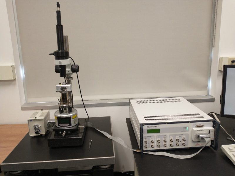 Atomic Force Microscopy
Atomic force microscopy (AFM) is a very-high-resolution type of scanning probe microscopy (SPM), with demonstrated resolution on the order of fractions of a nanometer, more than 1000 times better than the optical diffraction-limit.
-
General Item
 BET (Brunauer–Emmett–Teller)
Brunauer–Emmett–Teller (BET) theory is used to measure the surface area of solid or porous materials. It gives important information on their physical structure as the area of a material’s surface affects how that solid will interact with its environment. Many properties such as dissolution rates, catalytic activity, moisture retention, and shelf life are often correlated to a material’s surface area. Critical to the design and manufacture of solids, surface area analysis is one of the most widely used methods in material characterization.
-
General Item
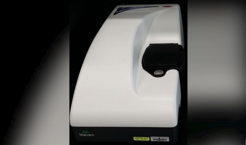 Dynamic Light Scattering
Dynamic light scattering (DLS) measures the time dependent fluctuations in the scattering intensity to determine the translational diffusion coefficient, and subsequently the hydrodynamic diameter from the Stokes-Einstein equation.
-
General Item
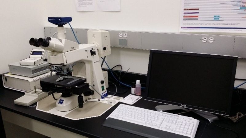 Fluorescence Microscopy
A fluorescence microscope is an optical microscope that uses fluorescence instead of, or in addition to, scattering, reflection, and attenuation or absorption, to study the properties of organic or inorganic substances.
-
General Item
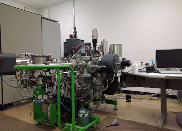
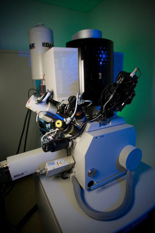 Focused Ion Beam
Dual beam FIB-SEM is a workstation that combines a scanning electron microscope (SEM) and a focused ion beam (FIB); it is heavily used in semiconductor industry, materials science, and increasingly in geoscience and biological field for site-specific analysis. SEM delivers high resolution images, while FIB is mostly used to add and subtract micro volumes of material in a controlled manner, like a nanomachining device. Coupled to an Energy Dispersive X-ray Spectroscopy (EDS) detector and Electron Backscattered diffraction (EBSD) camera, dual beam FIB-SEM provides elemental identification and crystallographic properties from the cross-section of the sample. With serial slicing technique, structural, chemical and crystallographic information can be revealed in three dimensions.
-
General Item
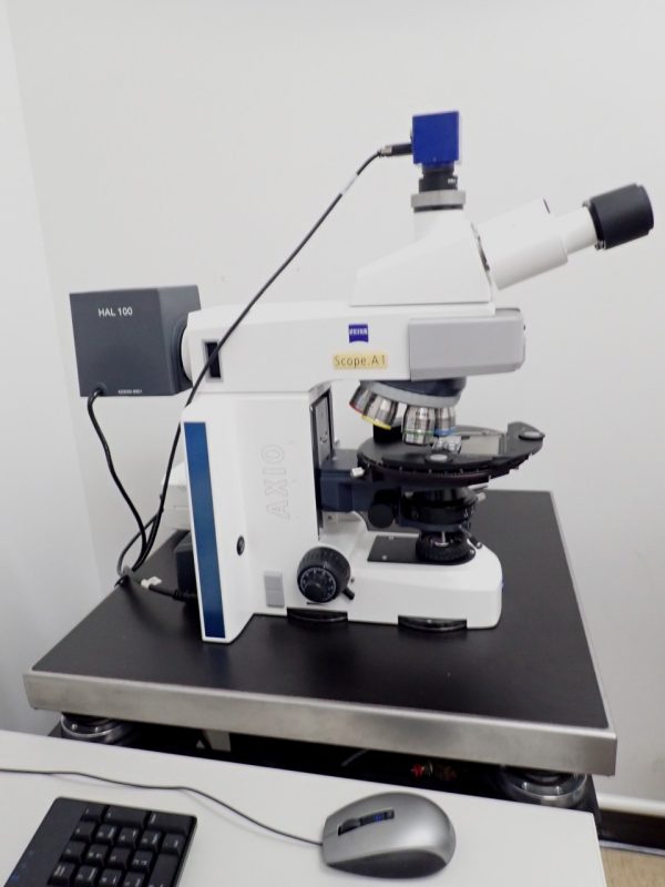 Optical Microscopy
The optical microscope, also referred to as a light microscope, is a type of microscope that commonly uses visible light and a system of lenses to generate magnified images of small objects. Optical microscopes are the oldest design of microscope and were possibly invented in their present compound form in the 17th century. Basic optical microscopes can be very simple, although many complex designs aim to improve resolution and sample contrast. The object is placed on a stage and may be directly viewed through one or two eyepieces on the microscope. In high-power microscopes, both eyepieces typically show the same image, but with a stereo microscope, slightly different images are used to create a 3-D effect. A camera is typically used to capture the image (micrograph). The sample can be lit in a variety of ways. Transparent objects can be lit from below and solid objects can be lit with light coming through (bright field) or around (dark field) the objective lens. Polarised light may be used to determine crystal orientation of metallic objects. Phase-contrast imaging can be used to increase image contrast by highlighting small details of differing refractive index. A range of objective lenses with different magnification are usually provided mounted on a turret, allowing them to be rotated into place and providing an ability to zoom-in. The maximum magnification power of optical microscopes is typically limited to around 1000x because of the limited resolving power of visible light. The magnification of a compound optical microscope is the product of the magnification of the eyepiece (say 10x) and the objective lens (say 100x), to give a total magnification of 1,000×. Modified environments such as the use of oil or ultraviolet light can increase the magnification.
-
General Item
 Particle Sizer/Counter
Aerosol monitors, commonly referred to as dust monitors, particulate monitors, light scattering laser photometers, are used to measure dust, smoke, mist, fume, condensates, and fog, and offer real-time, direct-reading results, which is quickly becoming an industry best practice in occupational hygiene, indoor air quality, and outdoor environmental fugitive emissions monitoring.
-
General Item
 Raman Spectroscopy
Raman Spectroscopy is a non-destructive chemical analysis technique which provides detailed information about chemical structure, phase and polymorphy, crystallinity and molecular interactions. It is based upon the interaction of light with the chemical bonds within a material. Raman is a light scattering technique, whereby a molecule scatters incident light from a high intensity laser light source. Most of the light is scattered at the same wavelength as the laser source and does not provide useful information – this is called Rayleigh Scattering. However a small amount of light (typically less than 1 in 1 million incident photons) is scattered at different wavelengths, which depend on the chemical structure of the analyte – this is called Raman Scattering which occurs in two ways. If the scattered light is of lower frequency (longer wavelength) than the incident laser, then it is called Stokes scattering. If it is of higher frequency (shorter wavelength), then it is called anti-Stokes scattering. Most Raman spectroscopy detects the more intense Stokes scattering.
-
General Item
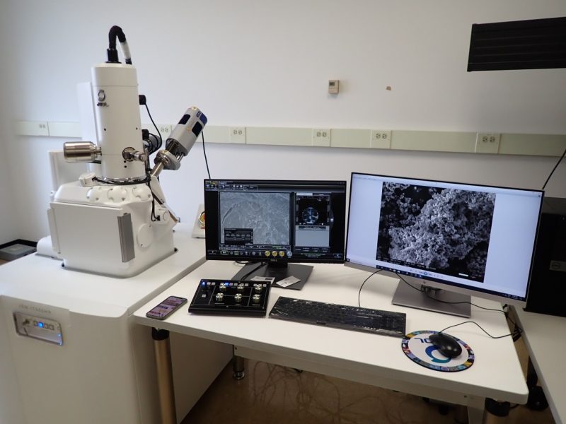 Scanning Electron Microscopy
Scanning electron microscope (SEM) is widely used to characterize the sample surface and near-surface. It provides high resolution images, and elemental microanalysis in conjunction with an Energy Dispersive X-ray Spectroscopy (EDS) detector. With specialized instruments and compartments, SEM may have variable pressure or environmental capabilities that specimens can be observed in high vacuum, low vacuum or wet condition; in-situ experiments such as hydrating, dehydrating and sample heating are also possible.
-
General Item
 Secondary Ion Mass Spectrometry
Secondary-ion mass spectrometry (SIMS) is a technique used to analyze the composition of solid surfaces and thin films by sputtering the surface of the specimen with a focused primary ion beam and collecting and analyzing ejected secondary ions. The mass/charge ratios of these secondary ions are measured with a mass spectrometer to determine the elemental, isotopic, or molecular composition of the surface to a depth of 1 to 2 nm. Due to the large variation in ionization probabilities among elements sputtered from different materials, comparison against well-calibrated standards is necessary to achieve accurate quantitative results. SIMS is the most sensitive surface analysis technique, with elemental detection limits ranging from parts per million to parts per billion.
-
General Item
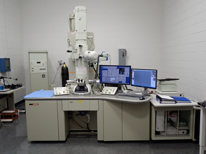 Transmission Electron Microscopy
The transmission electron microscope (TEM) is ideal for studying the defect microstructures of crystals, and probably no other single instrument has contributed more to our understanding of the nature of crystal defects and of microstructurally related properties of a wide range of crystalline materials. In addition to the usual imaging and electron diffraction facilities, most modern microscopes for materials science research are equipped with an x-ray energy dispersive spectrometer (EDS) for chemical analysis of very small regions of specimen. Thus, modern transmission electron microscopy (also TEM) can be considered as a logical development from {optical microscopy, x-ray crystallography, and electron microprobe analysis} techniques with which most mineralogists and geologists are familiar. From “Transmission Electron Microscopy of Minerals and Rocks” by Alex C. McLaren.
-
General Item
 UV-Vis Spectroscopy
UV-Vis spectrophotometer is a powerful analytical technique to determine the optical properties (transmittance and absorbance). It is generally used to determine analyte concentrations or the chemical conversion of a component in solution, and measure the transmittance of a solid sample.
-
General Item
 X-ray Diffraction
X-ray crystallography (XRC) is the experimental science determining the atomic and molecular structure of a crystal, in which the crystalline structure causes a beam of incident X-rays to diffract into many specific directions. By measuring the angles and intensities of these diffracted beams, a crystallographer can produce a three-dimensional picture of the density of electrons within the crystal. From this electron density, the mean positions of the atoms in the crystal can be determined, as well as their chemical bonds, their crystallographic disorder, and various other information.
-
General Item
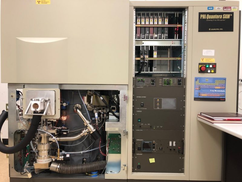 X-ray Photoelectron Spectroscopy
X-ray Photoelectron Spectroscopy (XPS) also known as Electron Spectroscopy for Chemical Analysis (ESCA) is a surface analysis technique, used for quantitative analysis of the chemical elements and chemical states from the surface of the material being studied. The average depth of analysis for an XPS measurement is approximately 5 nm. XPS can also be used to obtain depth distribution information by combining XPS measurements with ion milling (sputtering) to characterize thin film structures.
Still have questions?
Contact us and we'll chat with you about your specific research project and make recommendations on how to proceed.