

Scanning Electron Microscopy
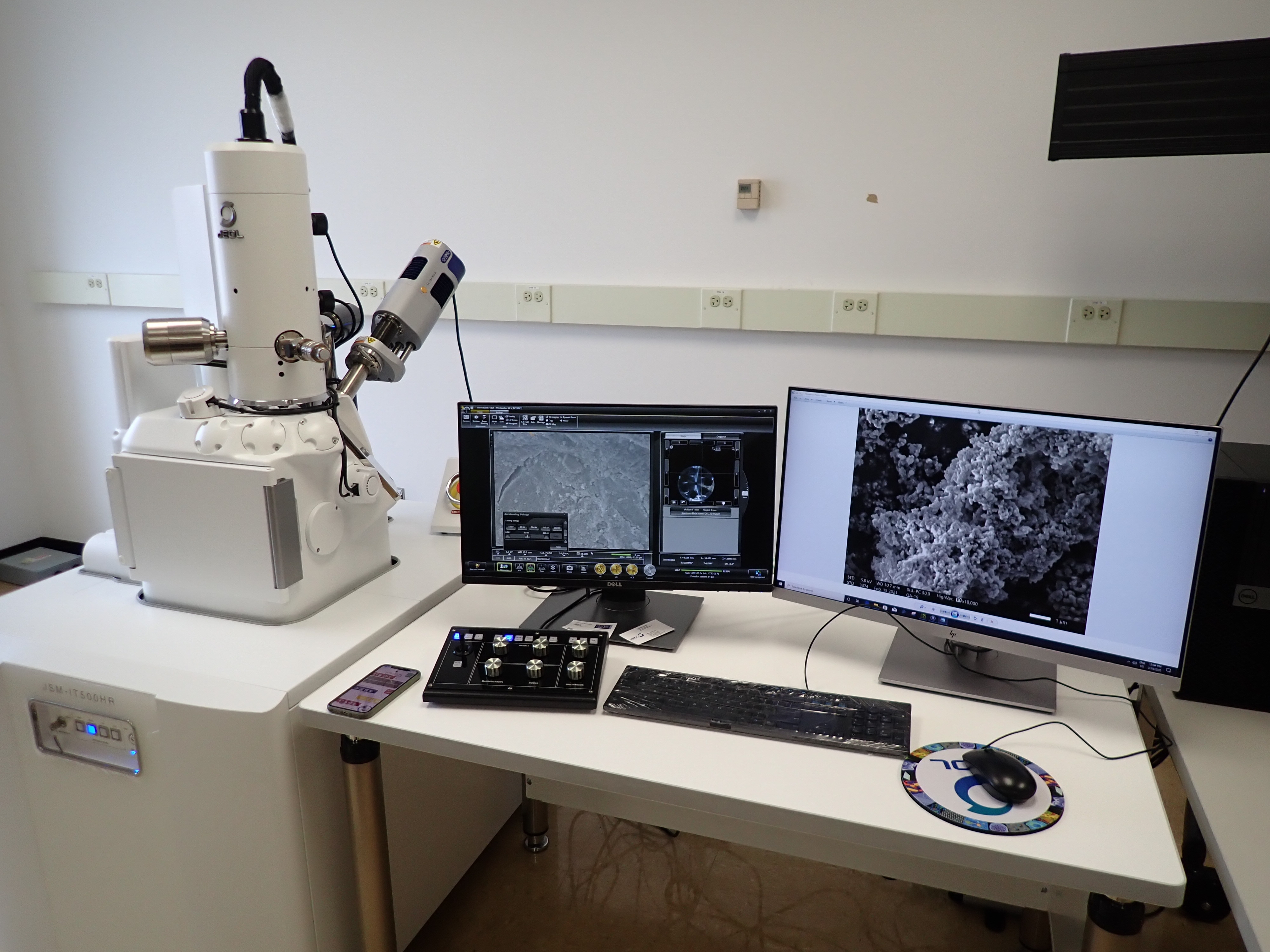
Scanning electron microscope (SEM) is widely used to characterize the sample surface and near-surface. It provides high resolution images, and elemental microanalysis in conjunction with an Energy Dispersive X-ray Spectroscopy (EDS) detector. With specialized instruments and compartments, SEM may have variable pressure or environmental capabilities that specimens can be observed in high vacuum, low vacuum or wet condition; in-situ experiments such as hydrating, dehydrating and sample heating are also possible.
APPLICATIONS
- High resolution imaging of surface topography
- Chemical analysis of nearly the entire period table
- Imaging of insulating and hydrated samples in certain mode
- In-situ experiments such as hydrating, dehydrating and heating
LIMITATIONS
- Sample size restriction
- Ultimate resolution is affected by the sample chemical and stability in the electron beam
Capability: Electron Backscatter Diffraction (EBSD)
Electron backscatter diffraction (EBSD) is a scanning electron microscope–based microstructural-crystallographic characterization technique commonly used in the study of crystalline or polycrystalline materials. The technique can provide information about the structure, crystal orientation, phase, or strain in the material. Traditionally these types of studies have been carried out using X-ray diffraction (XRD), neutron diffraction and/or electron diffraction in a Transmission electron microscope.